光製品Navi運営へのお問合せ

AEMtec GmbH

住所 〒12489
James-Franck-Str. 10 Berlin Germany
TEL 49-30-6392-7300
FAX 49-30-6392-7302
URL http://www.aemtec.com/
E-mail
  最終更新日:2022年03月24日

企業PR

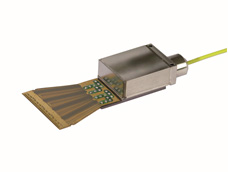
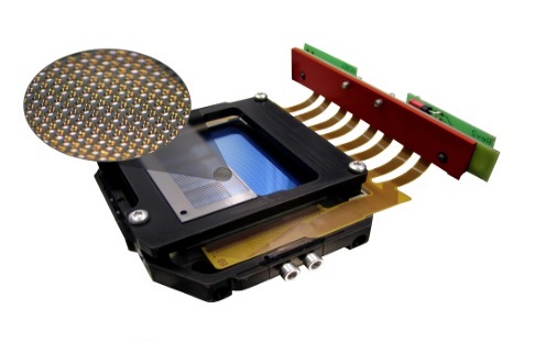
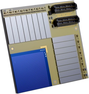
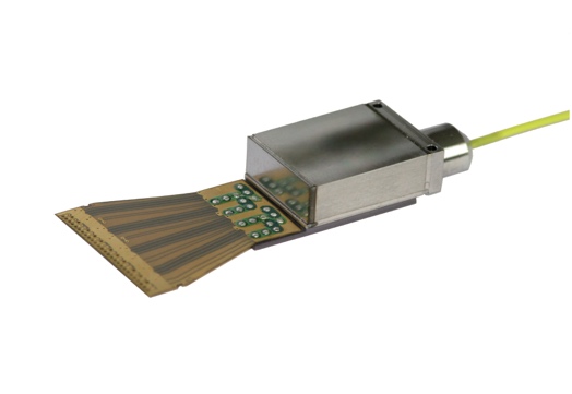
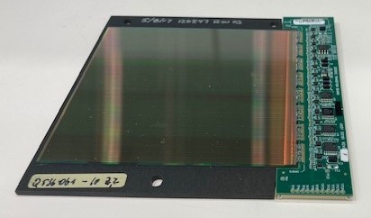
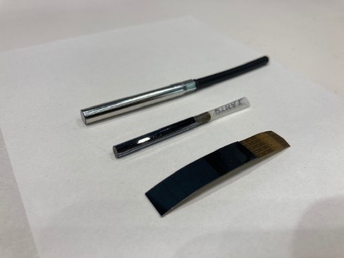
AEMtecは、ハイエンド・チップレベル技術を用いたハイエンド・カスタマイズ・マイクロシステム、オプトエレクトロニクス、センサーシステムの開発・生産において、お客様の信頼できる技術パートナーです。

取扱海外企業

  • AEMtec GmbH

AEMtec GmbH 取り扱い製品

Micromirror Assembly : Highly Complex Micromirror Assembly

Micromirror Assembly : Highly Complex Micromirror Assembly

Services
Feasibility Study • Layout and Design • Prototyping • Life Time Testing • Thermal-Mechanical Simulation (Finite Element Method FEM) • Industrialization
Technologies
60 x 60 x 5 mm³ / 60 g • All ICs mounted as Flip Chips • 28 x 28 mm MEMS mirror array • 29 layer ceramic substrate

資料請求する

Data Communication Module: Multi-Channel Optical Transceiver

Data Communication Module: Multi-Channel Optical Transceiver

Services
Feasibility Study • Chip-Design Support • Layout and Design • Package Technology • Design Support • Thermal Simulation
Technology
Flex Soldering • Placement Accuracy of Photodiode ± 1µm • Dicaps & Chipresistors Accuracy of ± 20µm • Exact Wire Bond Loops, 23µm wire

資料請求する

VCSEL Module

VCSEL Module

Services
Packaging Technology • Life Time Testing • Thermal-Mechanical
Simulation (Finite Element Method FEM) • Industrialization
Technologies
64x64 VCSELs • Lens array to focus the beams glued with UV-glue • Glass substrate with 2 alignment marks at each VCSEL position • VCSEL dimensions 0.2x0.2x0.15mm³

資料請求する

Micromirror Assembly : Highly Complex Micromirror Assembly

Micromirror Assembly : Highly Complex Micromirror Assembly

Services
Feasibility Study • Layout and Design • Prototyping • Life Time Testing • Thermal-Mechanical Simulation (Finite Element Method FEM) • Industrialization
Technologies
60 x 60 x 5 mm³ / 60 g • All ICs mounted as Flip Chips • 28 x 28 mm MEMS mirror array • 29 layer ceramic substrate

資料請求する

Data Communication Module: Multi-Channel Optical Transceiver

Data Communication Module: Multi-Channel Optical Transceiver

Services
Feasibility Study • Chip-Design Support • Layout and Design • Package Technology • Design Support • Thermal Simulation
Technology
Flex Soldering • Placement Accuracy of Photodiode ± 1µm • Dicaps & Chipresistors Accuracy of ± 20µm • Exact Wire Bond Loops, 23µm wire

資料請求する

VCSEL Module

VCSEL Module

Services
Packaging Technology • Life Time Testing • Thermal-Mechanical
Simulation (Finite Element Method FEM) • Industrialization
Technologies
64x64 VCSELs • Lens array to focus the beams glued with UV-glue • Glass substrate with 2 alignment marks at each VCSEL position • VCSEL dimensions 0.2x0.2x0.15mm³

資料請求する

Micromirror Assembly

Micromirror Assembly

Highly Complex Micromirror Assembly
Services
Feasibility Study • Layout and Design • Prototyping • Life Time Testing • Thermal-Mechanical Simulation (Finite Element Method FEM) • Industrialization
Technologies
60 x 60 x 5 mm³ / 60 g • All ICs mounted as Flip Chips • 28 x 28 mm MEMS mirror array • 29 layer ceramic substrate

資料請求する

Data Communication Module

Data Communication Module

Multi-Channel Optical Transceiver
Services
Feasibility Study • Chip-Design Support • Layout and Design • Package Technology • Design Support • Thermal Simulation
Technology
Flex Soldering • Placement Accuracy of Photodiode ± 1µm • Dicaps & Chipresistors Accuracy of ± 20µm • Exact Wire Bond Loops, 23µm wire

資料請求する

VCSEL Module

VCSEL Module

Services
Packaging Technology • Life Time Testing • Thermal-Mechanical
Simulation (Finite Element Method FEM) • Industrialization
Technologies
64x64 VCSELs • Lens array to focus the beams glued with UV-glue • Glass substrate with 2 alignment marks at each VCSEL position • VCSEL dimensions 0.2x0.2x0.15mm³

資料請求する

Micromirror Assembly: Highly Complex Micromirror Assembly

Micromirror Assembly: Highly Complex Micromirror Assembly

主な機能
フィージビリティスタディ - レイアウト設計 - 試作 - ライフタイムテスト - 熱-機構シミュレーション(有限要素法FEM) - 量産化
テクノロジー
60 x 60 x 5 mm³ / 60 g - すべてのICをフリップチップで実装 - 28 x 28 mmのMEMSミラーアレイ - 29層セラミック基板

資料請求する

Data Communication Module: Multi-Channel Optical Transceiver

Data Communication Module: Multi-Channel Optical Transceiver

機能
フィージビリティスタディ - チップ設計支援 - レイアウト・設計 - パッケージ技術 - 設計支援 - 熱シミュレーション
技術情報
フレックスソルダリング - フォトダイオードの配置精度±1µm - ダイキャップとチップレジスターの配置精度±20µm - 正確なワイヤーボンドループ、23µmワイヤー

資料請求する

VCSEL Module

VCSEL Module

機能
パッケージング技術 - ライフタイムテスト - 熱-機構シミュレーション(有限要素法FEM) - 量産化
技術概要
64×64個のVCSEL ・UV接着剤で接着されたビームを集束するレンズアレイ ・各VCSELの位置に2つのアライメントマークがあるガラス基板 ・VCSELの寸法0.2×0.2×0.15mm³"

資料請求する

マイクロミラーアセンブリ

マイクロミラーアセンブリ

サービス内容
フィージビリティスタディ - レイアウトとデザイン - プロトタイピング - ライフタイムテスト - サーマルメカニカルシミュレーション(有限要素法FEM) - 製品化
技術内容
60 x 60 x 5 mm³ / 60 g - ICはすべてフリップチップで実装 - 28 x 28 mm MEMSミラーアレイ - 29層セラミック基板

資料請求する

VCSELモジュール

VCSELモジュール

サービス内容
パッケージング技術 - ライフタイムテスティング - サーマルメカニカル
シミュレーション(有限要素法FEM) - 産業化対応
技術紹介
64x64 VCSELs - ビーム集束用レンズアレイはUV接着剤で接着 - 各VCSEL位置に2つのアライメントマーク付きガラス基板 - VCSEL寸法 0.2x0.2x0.15mm³ - VCSEL寸法 0.2x0.2x0.15mm

資料請求する

大型CMOSセンサー

大型CMOSセンサー

サービス内容
フィージビリティスタディ - チップ設計支援 - レイアウト設計 - パッケージング技術
技術紹介
CMOSセンサーの高精度配置とキュアプロセス - 低チップディフレクションが必要 - 精密ワイヤボンドループ

資料請求する

超音波プローブ

超音波プローブ

サービス内容
フィージビリティスタディ - レイアウト・デザインサポート - パッケージング技術
技術紹介
フレックス基板に高精度でフリップチップを搭載 - 鉛フリーはんだ - 折り曲げ技術

資料請求する

データ通信モジュール

データ通信モジュール

サービス内容
フィージビリティスタディ - チップ設計支援 - レイアウト設計 - パッケージ技術 - 設計支援 - サーマルシミュレーション
技術紹介
フレックスソルダリング - フォトダイオードの配置精度±1µm - ダイキャップとチップ抵抗の配置精度±20µm - 精密ワイヤボンドループ、23µmワイヤ

資料請求する

ページの先頭へ