光製品Navi運営へのお問合せ

WaferPlus Technology Co., Ltd.

住所 〒-
3F., No. 8-6, Ln. 169, Kangning St., Xizhi Dist., New Taipei City 221013 Taiwan
TEL +886-2-2697-5222
FAX +886-2-2697-6122
URL https://www.waferplus.com.tw/
E-mail max@waferplus.com
設立年 1978年
資本金 24,900,000円
GM Max Huang
  最終更新日:2026年03月13日

OPIE '26 出展の見どころ

1. DNA and PCR sequencing.
2. SEMI 3D IC glass carrier wafer.
3. Optical packaging glass wafer.
4. MEMS packaging wafer.
5. Microfluidic glass channel, cavity, and micro-reactor.
6. Optical Diffuser.
7. LED, and OLED packaging Glass, Quartz, Silicon caps.
8. TGV glass wafer.

詳細はこちら

企業PR

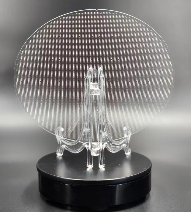
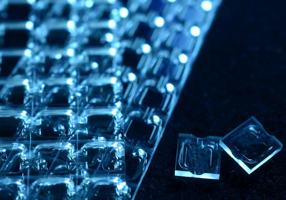
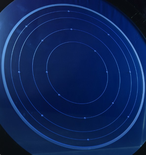
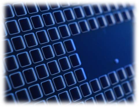
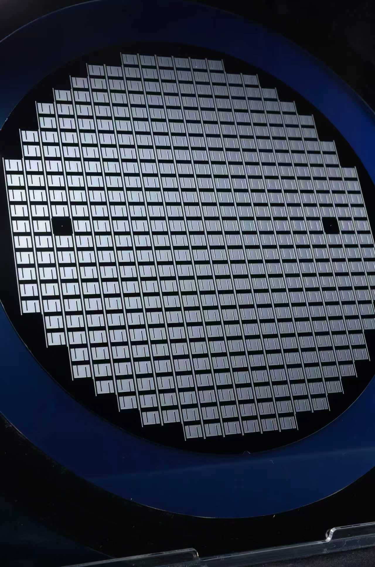
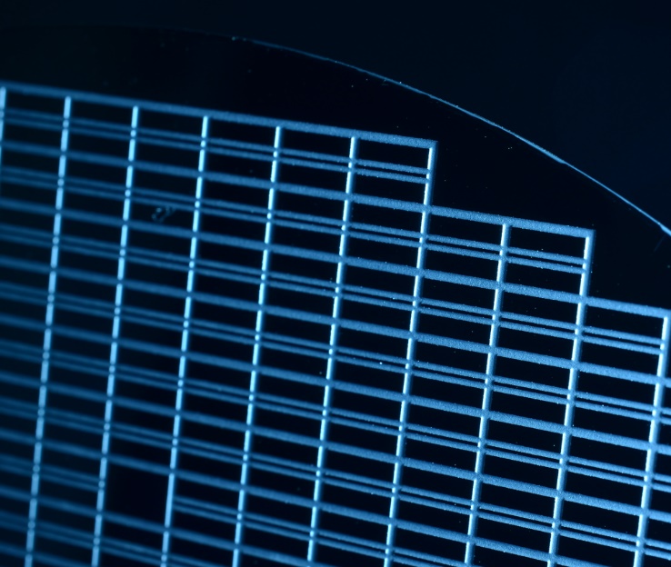
WaferPlus, starting from 1978, with factories located in China and Taiwan, a leading ISO 9001 and ISO 13485 certificated manufacturer, providing Cutting-edge solutions for products made by Glass, Quartz, Silicon, Sapphire, SiC, ALN, and Optical materials.
Focusing on SEMI, BIO, MEMS, Microfluidic, Electronic Packaging, Optic-electronics, LED, Display, WaferPlus utilizes the advanced processing capabilities with Laser Invisible Cutting, Laser Drilling (0 chipping), Laser Marking, CNC, Dry Etching, Wet Etching, Grinding + Polishing, Anodic Bonding, Laser Direct Bonding, Glue Bonding, Optical coating, Ultrasonic Washing with Cleanroom Class 100, offering product dimensions from Dia. 50mm
to Dia. 300mm based on Customized design.

WaferPlus Technology Co., Ltd. 取り扱い製品

Diffuser glass and quartz for Laser.

Diffuser glass and quartz for Laser.

Customized diffusing angles on glass, quartz and sapphire for various applications such as Laser, VCSEL and IR.

資料請求する

TGV glass wafer by Laser-Induced Etching (LIE)

TGV glass wafer by Laser-Induced Etching (LIE)

For TGV,low to high CTE glasses in size @ 4”, 6”, 8“, and 12“ are available.
Thin glass 100um with fine hole drilling Dia. 30um.

資料請求する

Laser, LED, and OLED packaging Glass, Quartz, Silicon caps.

Laser, LED, and OLED packaging Glass, Quartz, Silicon caps.

Packaging cap for UVA, UVC, UHB LEDs used in Automotive, Projection, Stage lighting, IR sensing, OLED lighting, OLED Display etc.

資料請求する

DNA and PCR sequencing: Low-Fluorescence glass and quartz chip

DNA and PCR sequencing: Low-Fluorescence glass and quartz chip

1. Low-phosphor glass and quartz as substrate
2. Customized DNA and PCR sequencing solutions based on glass.

資料請求する

SEMI 3D IC glass carrier wafer

SEMI 3D IC glass carrier wafer

1. Wafer Diameter : 2inch (50mm) to 12inch(300mm). Round, Square, and Customized shape upon request.
2. Thickness: 50µm ~ 3000µm.
3. TTV < 1 µm.
4. Roughness (Ra) < 0.5 nm (5A).
5. Surface treatment: Polished or Frosted.
6. Laser Marking available.

資料請求する

Optical packaging glass wafer with optical cavity

Optical packaging glass wafer with optical cavity

1. Micro-structuring on wafers and substrates with cavities, blind hole, through hole and groove.
2. Hole diameter: Dia. 30 µm (0.03mm).
3. Cavity depth: 5 µm (0.005mm) with Clear or Frosted bottom.
4. Groove: 10 µm (0.01mm).

資料請求する

MEMS packaging wafer made by Tempax

MEMS packaging wafer made by Tempax

Micro-structuring on wafers and substrates with holes and cavities.
1. Hole diameter: Dia. 30 µm (0.03mm).
2. Cavity depth: 5 µm (0.005mm) with Clear or Frosted bottom.
3. Groove: 10 µm (0.01mm).

資料請求する

Microfluidic glass channel, cavity, and micro-reactor

Microfluidic glass channel, cavity, and micro-reactor

1. Structuring for optical cavities, tunnels, blind hole, through holes.
2. Glue bonding for Microfluidic chips.
3. Anodic bonding for silicon and glass wafer.

資料請求する

ページの先頭へ